


 EMERGING TECH
EMERGING TECH
EMERGING TECH
EMERGING TECH
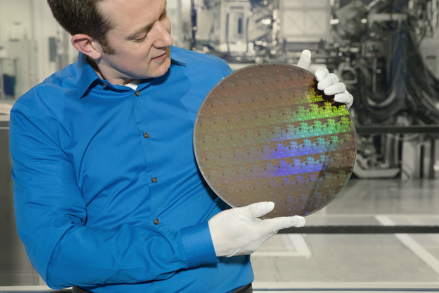
While chip market leader Intel Corp. is only just starting to experiment with transistors that are 7 nanometers thick, a consortium led by IBM Corp. has already reached the next evolutionary stage of semiconductor technology. Engineers from the company’s research arm, Samsung Electronics Co. Ltd. and GlobalFoundries Inc. are currently testing the world’s first batch of even thinner 5-nm chips.
The processors are the fruit of a years-long development effort orchestrated at the SUNY college network’s NanoTech Complex in Albany, New York. They were created using a novel fabrication method that marks a departure from the finFET technology on which current chips are based. Instead of the conventional flat rectangular structure, the individual transistors are produced in a vertical configuration that provides more room for components.
That provides several logistical benefits. The biggest is that each transistor can be equipped with four of the logistical gates that do the heavy lifting on a chip rather than three like in finFET-based designs. According to IBM, the increased density yields an improvement across several important criteria.
First, the technology provides the ability to squeeze up to 30 billion transistors on a 50-square-millimeter chip compared with the 20 billion possible with 7nm technology. The difference becomes even more noticeable when using the 10nm processors already available on the market as the benchmark. IBM claims that its 5-nm design can run 40 percent faster than a 10nm system, or alternatively, use 75 percent less electricity to provide the same performance.
In more practical terms, this means that a smartphone with a 5-nm chip could last two to three days on a single charge. The technology is still in early stages, but consumers can expect it to appear in their devices much sooner than the more exotic types of chips that IBM is developing. The company believes that commercial production could start as early as 2019 thanks to the fact that the architecture employs many of the same building blocks as current processors.
Reaching the 5-nm mark would represent a major victory not only for semiconductor makers but the technology industry as a whole. Many of today’s most important trends, including artificial intelligence, can be credited at least partially to the fact that researchers and developers have seen a rapid increase in the amount of computing power available at their disposal over recent years. Further improvements in processing density hold the potential to bring about even more significant advances.
And for IBM, it’s an opportunity to open valuable new revenue streams. Together with AI, the company’s chip development efforts form a key part of its plan to offset the declines in its legacy product lines.
… We’d like to tell you about our mission and how you can help us fulfill it. SiliconANGLE Media Inc.’s business model is based on the intrinsic value of the content, not advertising. Unlike many online publications, we don’t have a paywall or run banner advertising, because we want to keep our journalism open, without influence or the need to chase traffic.The journalism, reporting and commentary on SiliconANGLE — along with live, unscripted video from our Silicon Valley studio and globe-trotting video teams at theCUBE — take a lot of hard work, time and money. Keeping the quality high requires the support of sponsors who are aligned with our vision of ad-free journalism content.
If you like the reporting, video interviews and other ad-free content here, please take a moment to check out a sample of the video content supported by our sponsors, tweet your support, and keep coming back to SiliconANGLE.